
PCB design in practice: what actually decides whether a board works
Stack-up, placement, power distribution, thermal behaviour and manufacturability. The schematic says what is connected; the layout decides whether it works.
In short
- The stack-up comes first. It sets cost, impedance and return paths, and changing it later means redoing the routing.
- Placement matters more than routing. A good placement makes routing easy; a poor one cannot be rescued by it.
- Decoupling is about loop area, not capacitance value.
- A review before fabrication is the highest-value hour in the project, because everything is still free to change.
- Expect two or three prototype revisions. Planning for one is what makes schedules slip.
What board design actually decides
A schematic says what is connected. The board decides whether it works. Emissions performance, thermal behaviour, noise on sensitive measurements, whether the product can be assembled efficiently, whether faults can be found in production, and a meaningful share of unit cost are all determined during layout rather than during circuit design.
That makes layout the point at which a design becomes real, and the point at which decisions become expensive to reverse. A schematic change is an afternoon. A layout change after fabrication is a new board, new assembly, and whatever testing the change invalidates.
Decided before anything is placed
Several things constrain the whole layout and belong at the start.
- Board outline and mounting. Where it fits, how it is held, where connectors must align with an enclosure. Mechanical constraints are usually immovable and should be established before placement rather than discovered during it.
- Stack-up. Layer count, thicknesses and which layers carry planes.
- Whether impedance is controlled. This drives stack-up and fabrication cost, and should follow from a requirement rather than from habit.
- Which manufacturing capability to design to. Minimum track width, spacing and hole size determine which fabricators can build it and at what price.
- Thermal expectations. Which parts dissipate meaningfully and whether the enclosure provides airflow.
- Assembly constraints. Single or double sided, any through-hole parts, and whether the assembler has a preference.
Before the layout: the schematic deserves attention too
Layout gets the discussion, and a proportion of board problems originate earlier, in decisions that were made on the schematic and never questioned.
- Component selection. Availability, lifecycle status and whether a second source exists are engineering decisions with long consequences, not procurement details to settle later. A design built around a part with one manufacturer and a long lead time has a problem that layout cannot fix.
- Package choice. Determines board area, assembly difficulty, thermal behaviour and whether the part can be reworked. A physically smaller package is not automatically better, particularly at low volumes where hand rework may be necessary.
- Protection at every external interface. Anything a person or the outside world can reach will eventually receive a discharge or a miswired connection. Adding protection at the schematic stage costs a few components; adding it after a field failure costs a revision.
- Test provision. Deciding which nodes need to be observable, and providing for it, before the layout has consumed the space.
- Unpopulated options. Footprints for filtering, alternative parts or a different configuration cost nothing on a bare board and give you options when something unexpected appears. This is the cheapest insurance in hardware design.
- Clear, readable drawing. A schematic is read far more often than it is drawn, including by whoever debugs the product in five years. Logical grouping, consistent signal naming and notes explaining unusual choices are worth the time.
A schematic review before layout begins catches things that become much more expensive once the board exists, and it takes an hour.
The stack-up
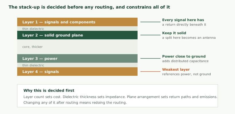
Two layers suit simple, slow designs with modest current. For anything containing a processor, four layers is the usual starting point, and the reason is not routing space but the pair of solid planes it provides.
The arrangement matters as much as the count. A signal layer immediately adjacent to a solid ground plane gives every trace on it a short, direct return path, which is what keeps loop area small and emissions low. The same signal layer with the plane two layers away has a worse return path and behaves accordingly. This is the mechanism discussed in EMC and compliance, and it is decided here.
A thinner dielectric between a signal layer and its reference improves that coupling, which is one reason a stack-up is specified rather than left to the fabricator’s default. Placing power and ground planes adjacent to each other adds useful distributed capacitance between them.
The weakness in a conventional four-layer arrangement is the bottom signal layer, which references power rather than ground. Signals there have a return path through the power plane, which works provided the plane is continuous and there is adequate capacitance between the planes, and works poorly otherwise. It is worth being aware of which of your signals live there.
Placement: the most consequential hour
Everything downstream depends on this, and it repays spending longer than feels comfortable.
A workable order, because each stage constrains the next:
- Mechanically fixed items first. Connectors that must align with an enclosure, mounting holes, anything with a physical constraint. These cannot move later.
- Then the switching converters. Their fast-current loops should be as small as possible, and placing them early means the loop is drawn deliberately rather than around whatever space remained.
- Then sensitive analogue and any radio. Away from switching circuits, with room for their own arrangement, as discussed in sensor selection and signal conditioning.
- Then the processor and its supporting parts, with decoupling positioned before routing rather than added afterwards.
- Then everything else, grouped by function so that related parts sit together and connections stay short.
The principle underneath is that placement should reflect the flow of the circuit. Power entering at one place and distributing outward; signals travelling from input to processing to output without crossing back; noisy and quiet regions separated by distance rather than by a cut in a plane.
The test of a good placement is that routing is mostly obvious. If routing is a struggle, the answer is usually to go back and move components rather than to route harder.
Power distribution
Getting power to parts reliably is unglamorous and causes a disproportionate share of difficult faults.
Decoupling is about loop area. A capacitor exists to supply fast current demands locally so they do not have to travel across the board. Its effectiveness depends on the size of the loop formed by the capacitor, the device pin it serves, and the plane. A capacitor placed close with short connections works; the same capacitor placed conveniently at the edge of a footprint with a longer path is much less effective, regardless of its value.
Size copper for the current. Track width and copper weight determine how much current a connection carries without excessive heating or voltage drop. Vias carry current too, and a single via in a high-current path is a common oversight; several in parallel are usually appropriate.
Think about where current actually flows. A plane is not an equipotential surface. Current takes particular paths through it, and a high-current path crossing an area serving sensitive circuitry will couple into it. Arranging the placement so power currents and sensitive circuits occupy different regions solves this without needing any cut in the plane.
Routing: what matters
Most connections need only to be short and sensible. A minority determine whether the board works, and identifying which is the skill.
- Keep the reference plane intact beneath fast signals. The single most common self-inflicted problem.
- Keep switching nodes short. The node between a switching device and its inductor carries the fastest voltage changes on the board and should be as small as it can be.
- Route differential pairs together, matched and consistently spaced, since their noise rejection depends on both conductors seeing the same environment.
- Separate noisy from sensitive by distance, and cross at right angles where crossing is unavoidable.
- Watch the layer changes. A signal changing layers needs its return current to change reference too, which requires a nearby via connecting the planes, or the return takes a long detour.
- Do not obsess over the rest. A slow signal routed reasonably will work. Time spent perfecting it is better spent on the handful that matter.
Mixed-signal boards, where most of the difficulty is
Boards carrying both a processor and sensitive measurement circuitry are where layout skill shows, because the two have directly conflicting requirements. The processor and its switching supply generate exactly the interference the measurement circuit must not see.
The approach that works is partitioning by placement rather than by cutting planes. Group the noisy circuitry in one region and the sensitive circuitry in another, physically separated, and let the reference plane remain continuous underneath both. Current then flows where the circuits are rather than across the board, and the plane continues to do its job for everything above it.
Several specifics follow from that.
- Do not route digital signals across the analogue region. A signal passing over a sensitive area couples into it regardless of which layer it is on.
- Keep the converter at the boundary. The analogue-to-digital converter sits between the two worlds, and placing it at the edge of the analogue region with its digital side facing the digital region keeps each signal in its own area.
- Separate the supplies. Filtering the analogue supply from the digital one, with a deliberate connection at a single considered point, keeps switching current out of the measurement reference without creating a plane split under signals.
- Watch where the noisy return current flows. A processor’s return current travelling through the region beneath an analogue circuit will couple into it even with an intact plane, which is an argument for the physical separation rather than against the plane.
- Keep the reference for the converter clean. Its accuracy is relative to that reference, so noise there appears directly in the measurement, as discussed in sensor selection and signal conditioning.
Where a design has genuinely demanding measurement requirements alongside a busy processor, it is worth considering whether they belong on the same board at all. Two boards with a considered interface between them is sometimes cheaper than the layout effort and the risk of combining them.
Thermal behaviour
Heat is frequently an afterthought and frequently what limits a design in service.
The board itself is the main heat spreader in most products. Copper conducts heat well, so connecting a dissipating component to a larger copper area, with vias carrying heat to planes and to the opposite side, is usually the primary cooling mechanism. This needs planning during placement, because it requires space.
Components should be derated: a part rated to a maximum temperature should not be operating close to it, because ambient rises, airflow may be worse than assumed, and lifetime falls as temperature rises. The enclosure matters too; a board that runs cool on a bench can be substantially hotter inside a sealed housing, which is why thermal verification should happen on the real assembly rather than on a bare board.
Separating heat sources helps. Two dissipating parts placed adjacent to each other create a hotspot that neither would produce alone, and moving them apart costs nothing at layout.
Mechanical integration, where surprises live
A board does not exist in isolation, and the interface between electronics and mechanics produces a recognisable set of problems.
- Connector alignment. A connector that must protrude through an enclosure has to be positioned within the tolerance stack of the board, its mounting, and the housing. Nominal alignment on a drawing does not guarantee that every unit assembles, and this is one of the most common causes of a production problem that did not appear on prototypes.
- Component height. Tall parts under a lid, or beneath another board, need clearance that has been checked rather than assumed. Electrolytic capacitors, connectors and shields are the usual offenders.
- Board thickness and flex. A thin board in a large area flexes during assembly and in service, which stresses joints on rigid components. Support points matter, particularly near connectors that will be repeatedly plugged.
- Mounting and grounding. How the board is held determines the mechanical stress it experiences and, where a metal chassis is involved, forms part of the electrical design, as discussed in EMC and compliance.
- Keepout regions. Areas under mounting bosses, near moving parts, or where a screw head sits need to be clear, and these constraints come from the mechanical side rather than the electrical one.
- Cable routing inside the enclosure. Where internal cables run affects both assembly time and electrical behaviour, and a cable routed across a sensitive circuit during assembly can undo careful layout work.
The reliable way to avoid these is a three-dimensional check of the assembled product before fabrication, with the real enclosure geometry rather than a nominal outline. This is straightforward with current tools and catches problems that are otherwise discovered by trying to close the lid on a prototype.
Documentation the manufacturer can build from
A manufacturing package that raises queries delays the build, and the queries are usually about the same handful of things.
| Item | Purpose | What its absence causes |
|---|---|---|
| Fabrication outputs and drill data | Building the bare board | Nothing proceeds |
| Fabrication drawing | Stack-up, material, finish, tolerances, special requirements | Assumptions that change impedance or finish |
| Bill of materials with approved alternates | Purchasing | Delays while substitutions are queried, or wrong parts fitted |
| Assembly drawing | Orientation, polarity, anything unusual | Components fitted the wrong way round |
| Pick and place data | Machine programming | Manual entry, with the errors that invites |
| Netlist | Verification against the fabricated board | Faults found later and more expensively |
| Notes on anything non-standard | Avoiding assumptions | The most common source of build queries |
Two additions repay the effort. A statement of which alternates are approved prevents both an unauthorised substitution and a line stopping while somebody seeks permission. And an explicit note about anything deliberate that looks like a mistake, such as an unpopulated footprint or an unusual clearance, prevents a well-intentioned query or correction.
Reliability, which is decided here too
A board that works on a bench and fails after two years in service has usually been let down by something in the layout rather than in the circuit.
- Mechanical stress on joints. Rigid components on a flexing board experience repeated stress at their solder joints. Larger parts, connectors and anything mounted near a fixing point are most affected. Support and placement away from flex points matter more than the joint itself.
- Thermal cycling. Expansion differences between a component and the board work joints over thousands of cycles. This is why a product cycling daily between temperature extremes fails differently from one running continuously warm.
- Vibration. Heavy components need mechanical support rather than relying on their joints. A tall capacitor or a connector taking cable loads should be secured.
- Contamination and moisture. Residues combined with humidity cause slow leakage and eventually corrosion, particularly between closely spaced conductors at different potentials. Cleanliness after assembly, and conformal coating where the environment warrants it, address this.
- Creepage and clearance. Where voltages are high enough to matter, physical spacing between conductors is a safety requirement as well as a reliability one, and it constrains layout in ways that must be respected rather than optimised away.
Most of these cost nothing to accommodate during placement and cannot be retrofitted. They are also the failures that appear after the product has shipped in volume, which makes them the most expensive kind to discover.
Design for manufacture
A board that is difficult to build costs more and yields worse, and most of it is straightforward to avoid.
- Consistent orientation for similar parts, which speeds placement and makes inspection easier.
- Adequate spacing between components, for placement accuracy, inspection access and rework.
- Balanced thermal connections on small parts, so that one end does not heat faster than the other and lift the component during reflow.
- Avoid the finest features available unless required, since they raise cost and reduce the number of fabricators who can build the board.
- Fiducials for placement alignment, and adequate clearance around the board edge.
- Panelisation planned with the assembler, including how boards will be separated and whether that stresses components near the edge.
- Clear polarity and pin-one markings that survive assembly and are visible for inspection.
Most of this is codified in the design rules your fabricator and assembler publish, and the single most useful action is to obtain those before starting rather than designing and then discovering.
Board types beyond the standard rigid board
Most products use a conventional rigid board, and a few situations justify something else. Each brings cost and constraints that are worth knowing before the mechanical design assumes one.
| Type | Suits | Costs |
|---|---|---|
| Standard rigid | Almost everything | Nothing unusual |
| Flexible | Fitting a curved space, or a connection that must move | Higher cost, needs careful bend design, harder to assemble |
| Rigid-flex | Replacing connectors and cables between sections | Substantially higher cost; fewer fabricators; worth it for reliability or space |
| Heavy copper | High current distribution | Affects feature sizes and cost; constrains fine-pitch parts |
| Metal core | High power dissipation, particularly lighting | Different thermal and assembly behaviour; usually single layer |
| High-frequency laminate | Radio designs at higher frequencies | Material cost; fewer suppliers; particular handling |
The case for rigid-flex is worth stating because it is frequently dismissed on cost alone. Replacing a connector pair and a cable assembly removes several parts, an assembly operation, and a common failure point, since connectors and cables are among the most frequent causes of field faults. Compared against that whole cost rather than against a bare board price, it is sometimes the cheaper answer, particularly in products subject to vibration.
Design for test
Whether faults can be found cheaply is decided here, and it interacts directly with production cost as discussed in product cost reduction.
Test points on supply rails and key nodes, accessible from one side where possible, make in-circuit testing feasible. Partitioning the circuit so subsystems can be exercised independently makes diagnosis faster. A means for firmware to report internal state, discussed in embedded firmware practice, frequently replaces a great deal of physical probing.
It is also worth ensuring that a board can be powered and partially tested before everything is assembled, so that a fault in one area does not prevent checking another.
The review before fabrication
This is the highest-value hour in a hardware project. Everything is still changeable, nothing has been paid for, and the cost of finding a problem here is a rearrangement rather than a revision.
A useful review covers: whether reference planes are continuous under fast signals; whether switching loops are as small as they can be; whether decoupling is placed close with short connections; whether protection and filtering sit at connectors rather than further in; whether high-current paths have adequate copper and vias; whether heat has somewhere to go; whether the mechanical constraints are actually met; whether the fabricator’s rules are satisfied; whether test access exists; and whether anything unusual is explained in the notes.
It should be done by someone who did not do the layout. The person who drew it knows what they intended, which is precisely what prevents them seeing what they actually did.
A pre-fabrication checklist
Rather than a general instruction to review carefully, the following is what we actually look for. It is not exhaustive and it catches most of what matters.
| Area | Check |
|---|---|
| Planes | Continuous beneath every fast signal; no unintended splits; layer changes have a nearby plane connection |
| Power | Track widths and via counts adequate for the current; decoupling close with short connections |
| Switching converters | Fast-current loop as small as achievable; input filtering present; switching node compact |
| Interfaces | Protection and filtering at the connector, not further in; return path for protection is short |
| Thermal | Dissipating parts have copper area and vias; heat sources separated; enclosure airflow considered |
| Mechanical | Connector positions verified against the real enclosure; heights checked; keepouts respected |
| Manufacturability | Fabricator rules satisfied; spacing adequate; orientation consistent; fiducials present |
| Test | Supply rails and key nodes accessible; subsystems independently exercisable |
| Documentation | Stack-up specified; unusual requirements noted; alternates approved; revision marked on the board |
| Sanity | Footprints verified against datasheets; polarity marked; pin one unambiguous |
The last row deserves emphasis because footprint errors are both common and expensive. A component footprint taken from a library rather than verified against the specific part’s datasheet is one of the most reliable ways to produce a board that cannot be assembled. Checking every footprint against the actual part being ordered, particularly pin numbering and orientation, is tedious and repeatedly worth it.
Working with fabricators and assemblers
These relationships affect quality and cost more than most engineering decisions, and a little effort improves both.
Get their design rules before you start. Every supplier publishes capabilities and preferences, and designing to them from the beginning avoids the queries and compromises that arise when a design arrives near their limits.
Ask what they would change. An assembler looking at a design will often spot something that will slow their line or reduce yield. They are rarely asked, and the observation costs nothing.
Understand their tolerances. What a supplier can hold reliably, as opposed to what they list as a minimum, is a different number. Designing to the reliable figure rather than the headline one improves yield.
Treat queries as useful. A build query usually indicates genuine ambiguity in the documentation, and resolving it in the documents rather than in an email prevents the same question on the next build.
Visit if you can. An hour watching your board being built produces observations that no documentation review will, as discussed in product cost reduction.
How long a board design takes, and what drives it
Estimating hardware work is difficult, and the variation between a simple board and a demanding one is larger than people outside the discipline expect. A few factors dominate.
Component count and density. Not linearly. A board that is comfortably within its area is much quicker to lay out than one where everything must be packed, because in the second case every placement decision constrains several others.
Whether anything is fast. Signals requiring controlled impedance, matched lengths or particular topologies add work that ordinary routing does not.
Mixed signal content. A board with sensitive measurement alongside a processor takes considerably longer than either alone, for the partitioning reasons described above.
Mechanical constraint. A board with a free outline is far quicker than one that must fit a defined space with connectors at specified positions.
Parts you have not used before. Each unfamiliar component needs its footprint created and verified, its requirements understood, and its supporting circuitry designed. A design using entirely familiar parts moves much faster.
How settled the schematic is. Layout that begins before the circuit is stable is layout that will be redone.
The estimate that matters is rarely for the first version alone. Allowing for prototype revisions, and for the bring-up effort described above, produces a schedule that survives contact with reality. Presenting only the first-version figure is how hardware projects acquire a reputation for overrunning, when what actually happened is that the rest of the work was never in the plan.
First prototypes
Expect problems, and expect a proportion of them to be assembly errors rather than design faults.
The order of investigation matters. Verify supply rails before running anything, because a processor on a marginal or wrong rail produces symptoms indistinguishable from software faults. Then confirm the basics work before assuming the interesting parts are at fault.
Plan for more than one revision. Two or three is normal for competent teams on a new design, because first prototypes reveal interactions that no amount of review anticipates. A schedule assuming a single revision is not aggressive, it is optimistic, and it is the most common cause of hardware projects arriving late.
Keep a careful record of every modification made to prototypes. Cut tracks and added wires accumulate quickly, and reproducing them into the next revision depends on somebody having written them down.
Revisions, and keeping track of them
A board will change, several times before production and occasionally afterwards. How that is managed determines whether the history remains comprehensible.
Version everything together. Schematic, layout, bill of materials and firmware that depends on the hardware. A board revision with a bill of materials from a different version is a recognised way to build something that cannot work.
Mark the revision on the board itself. In copper or silkscreen, readable once assembled. When a unit returns from the field, knowing which revision it is saves a great deal of guessing, and the cost is nothing.
Record what changed and why. Not just that a component value moved, but the problem it addressed. Two years later somebody will consider reverting it, and the reason is what stops them.
Keep prototype modifications written down. Cut tracks and added wires accumulate during bring-up and are easy to forget. A revision that omits one of them reproduces a fault that was already solved.
Decide what a revision means for firmware. If a change alters a pin assignment or a peripheral, firmware must know which board it is running on, either by being built for it or by detecting it. A single firmware image that silently misbehaves on an older board is an unpleasant class of problem, and it connects directly to the version tracking discussed in device security and OTA updates.
When to stop revising
There is a point at which further improvement costs more than it returns, and recognising it is part of the discipline. A board that meets its requirements with adequate margin, can be built reliably, and has no known issues is finished, even if it could be smaller or cheaper. Continuing to optimise a working design delays production and introduces risk into something that already works.
The exception is anything found during compliance testing or reliability work, which should be addressed rather than accepted, because those findings indicate a real problem rather than an aesthetic one.
Mistakes worth avoiding
- Routing before placement is settled. The effort is wasted when components move.
- Splitting planes under fast signals. Creates the loop the plane existed to prevent.
- Decoupling placed for convenience. Loop area, not value, determines effect.
- Specifying controlled impedance without a requirement. Cost and constraint for nothing.
- Designing to the finest available features. Narrows suppliers and raises price.
- Leaving thermal until the prototype is hot. It needs space, which needs planning.
- No test access. Every production fault then costs more to find.
- Reviewing your own layout. You will see what you meant.
- Planning for one revision. Optimism disguised as a schedule.
What good looks like at handover
A board design that is genuinely finished comes with more than manufacturing outputs, and the difference shows when somebody else has to work on it.
- Design source files in a form that can be opened and edited, not only exported outputs. A design you cannot modify is a design you will eventually have to redraw.
- The library used, with footprints that were verified rather than assumed, so a future revision does not reintroduce a footprint error already found and fixed.
- Stack-up specification as built, including any impedance requirements and what was actually achieved.
- The constraint set: which rules were applied, which signals were treated as critical and why.
- Notes explaining anything unusual. A deliberate clearance, an unpopulated footprint, a component placed somewhere counter-intuitive for a reason.
- Test and bring-up findings from prototypes, including problems that were found and fixed, so they are not rediscovered.
- Known limitations, stated honestly. Every board has them.
The test of a handover is whether a competent engineer who has never seen the product can produce the next revision without archaeology. That is rarely true of a package consisting only of fabrication outputs, which is what a surprising number of handovers contain.
How we help
- Schematic and layout. Complete board design, from component selection through to manufacturing outputs.
- Stack-up and constraint definition, set against real requirements rather than defaults.
- Design review. On your design, before fabrication, where it is worth the most.
- Manufacturing package. Outputs, drawings, notes and data an assembler can build from without queries.
- Bring-up support. Getting first prototypes working, and distinguishing design faults from assembly ones.
- Revision work. Turning prototype findings into a design that can be built in volume.
The service page for this work is hardware and PCB design, and the route from concept to first working unit is described in idea to working prototype.
A short glossary
| Term | Meaning |
|---|---|
| Stack-up | The arrangement of copper and insulating layers through the thickness of the board. |
| Reference plane | A continuous copper layer providing the return path for signals on an adjacent layer. |
| Return path | The route current takes back to its source, which at high frequency is directly beneath the signal. |
| Loop area | The area enclosed by a current going out and returning. Small is better for both emissions and susceptibility. |
| Decoupling | Local capacitance supplying fast current demands so they need not travel across the board. |
| Controlled impedance | Trace geometry and stack-up specified so that signal paths present a defined impedance. |
| Via | A plated hole connecting layers. Carries current and has inductance, so quantity and placement matter. |
| Thermal via | A via used primarily to conduct heat away from a component into internal or opposite-side copper. |
| Fiducial | A marking used by assembly machines to align the board accurately. |
| Panelisation | Arranging several boards on one manufacturing panel, and how they are later separated. |
| Keepout | An area where components or copper must not be placed, usually for mechanical reasons. |
| Design rules | The minimum dimensions and clearances a fabricator can reliably achieve. |
If you take one thing away
The decisions that determine whether a board works are made early and quickly, often without anyone noticing they were decisions. The stack-up chosen from a default. The placement settled in an hour because routing was the interesting part. The decoupling positioned where there was room.
Each of those is nearly free to get right at the time and expensive to correct afterwards, because correcting any of them means a new board. That asymmetry is the whole argument for slowing down at the start: spending an extra day on stack-up and placement, and an hour on a review by someone who did not draw it, costs less than one avoidable revision.
And plan for revisions anyway. First prototypes reveal things that no review anticipates, and a schedule that allows for two or three is not pessimistic. It is the one that arrives on time. Where compliance testing sits in that schedule is covered in getting an electronic product certified. For the wider systems these boards end up in, see what industrial IoT actually is.
Questions we are asked about this
What clients ask before starting
How many layers do we need?
It depends on routing density, whether you need controlled impedance, and how much power the board distributes. Two layers suit simple low-speed designs; four is the usual starting point for anything with a processor, because it provides solid reference planes. More layers cost more and buy routing space and better electrical behaviour.
Why does placement matter more than routing?
Because placement determines how long connections have to be, where return currents flow, how heat spreads and whether the board can be assembled efficiently. A good placement makes routing straightforward; a poor one makes it impossible to route well no matter how much effort goes in afterwards.
Do we need controlled impedance?
Only where signal speeds or interface specifications require it. It constrains stack-up and adds fabrication cost. Many designs do not need it, and specifying it unnecessarily narrows your supplier options and raises price for no benefit.
How many prototype revisions should we expect?
More than one. Two or three is common even for competent teams, because first prototypes reveal things no amount of review finds. Planning for a single revision is what causes schedules to slip; planning for two or three usually means arriving on time.
What should be in the manufacturing package?
Fabrication outputs and drill data, a fabrication drawing with stack-up and finish specified, a bill of materials with approved alternates, assembly drawings showing orientation, pick and place data, and a netlist for verification. Clear notes about anything unusual prevent the queries that delay a build.
Can you review a design we already have?
Yes, and reviewing before fabrication is the single highest-value point to do it, because every option is still open and nothing has been paid for.
How do we keep the board cheap to build?
Fewer distinct parts, components on one side only where possible, no through-hole parts if avoidable, adequate spacing, and avoiding the finest manufacturing features unless the circuit genuinely requires them. This is covered in more depth in our guide to product cost reduction.
What causes most first-prototype failures?
In our experience, power problems and assembly errors rather than design logic. Verifying supply rails before running anything, and being willing to suspect the board rather than the firmware, resolves a large share of them quickly.
What are you designing?
Tell us what the board has to do, the environment it will work in, any mechanical constraints it must fit, and your expected volumes.